Voltage Regulators and Power Supplies » Step-Up/Step-Down Voltage Regulators » S8V9Fx Step-Up/Step-Down Voltage Regulators »
6V Step-Up/Step-Down Voltage Regulator S8V9F6

| Output voltage |
Typical max output current* |
Input voltage range | Size |
|---|---|---|---|
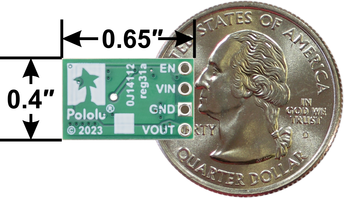
| 6 V | 1.5 A | 1.4 V – 16 V (2.7 V startup) |
0.4″ × 0.65″ |
*For input voltages close to the output. Actual achievable maximum continuous current is a function of input voltage and is limited by thermal dissipation. See the output current graphs on the product page for more information.
Alternatives available with variations in these parameter(s): output voltage Select variant…
 Compare all products in S8V9Fx Step-Up/Step-Down Voltage Regulators.
| Description | Specs (11) | Pictures (13) | Resources (3) | FAQs (0) | On the blog (0) | Distributors (37) |
|---|
Overview
 |
The S8V9Fx family of efficient switching regulators (also called switched-mode power supplies (SMPS) or DC-to-DC converters) convert both higher and lower input voltages to a regulated output voltage. They take input voltages from 1.4 V to 16 V and increase or decrease them as necessary, offering typical efficiencies of 80% to 90% and typical continuous output currents over 1 A for input voltages close to the output voltage. (Note: The minimum start-up voltage is 2.7 V; see the connections section for details.)
The flexibility in input voltage offered by this family of regulators is especially well-suited for battery-powered applications in which the battery voltage begins above the regulated voltage and drops below as the battery discharges. Without the typical restriction on the battery voltage staying above the required voltage throughout its life, new battery packs and form factors can be considered.
The S8V9Fx regulators have under-voltage lockout and over-current protection. A thermal shutdown feature also helps prevent damage from overheating and a soft-start feature limits the inrush current and gradually ramps the output voltage on startup.
This family consists of five regulators with output voltages ranging from 3.3 V to 9 V:
The different versions of the S8V9Fx regulators all look very similar, so the bottom silkscreen includes a blank space where you can add your own distinguishing marks or labels.
We manufacture these boards in-house at our Las Vegas facility, which gives us the flexibility to make these regulators with custom fixed output voltages. If you are interested in customization, please contact us.
 |
Details for item #4966
 |
Step-Up/Step-Down Voltage Regulator S8V9Fx, top view. |
|---|
Features
- Input voltage: 1.4 V to 16 V (Note: minimum start-up voltage is 2.7 V)
- Output voltage: 6 V with 4% accuracy
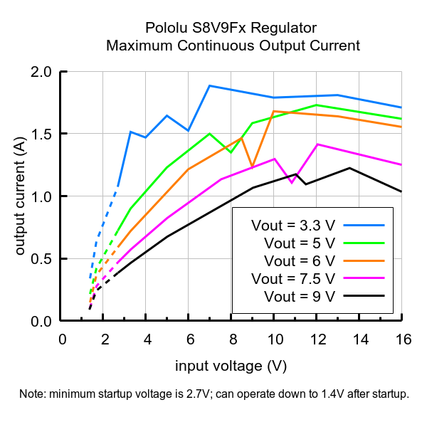
- Typical maximum continuous output current: 1 A to 1.5 A when input voltage is close to the output voltage (see the maximum continuous output current graph below for current capabilities across the full input voltage range)
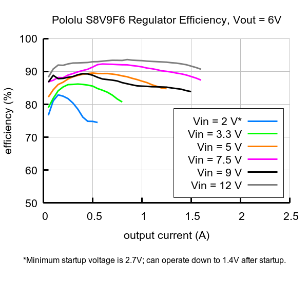
- Typical efficiency of 80% to 90%, depending on input voltage and load (see the efficiency graph below)
- Under 5 mA typical no-load quiescent current (see the quiescent current graph below); can be reduced to 10 µA to 15 µA per volt on VIN by disabling the board
- Soft-start feature limits inrush current and gradually ramps output voltage
- Over-current protection and over-temperature shutoff
- Input under-voltage lockout
- Power-saving feature maintains high efficiency at low currents
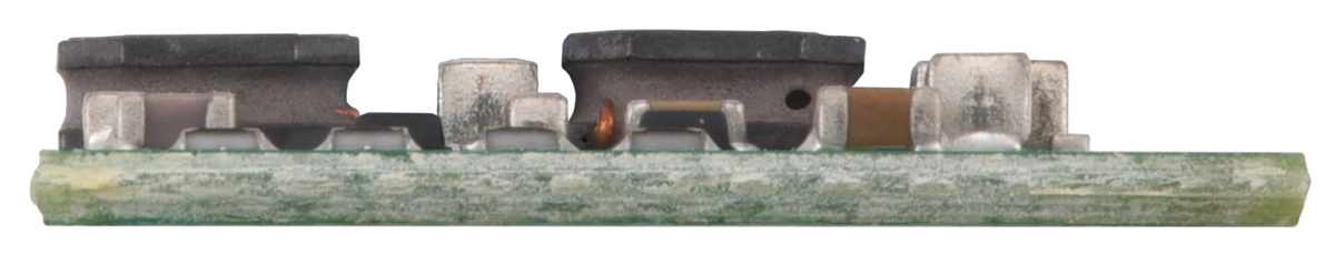
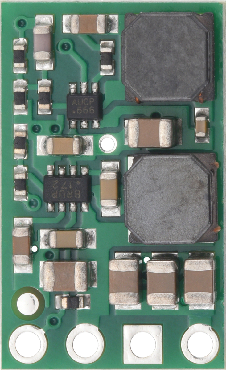
- Compact size: 0.4″ × 0.65″ × 0.1″ (10.2 mm × 16.5 mm × 2.6 mm); see the dimension diagram (719k pdf) for more information
Using the Regulator
Connections
The step-up/step-down regulator has four main connections: the output voltage (VOUT), ground (GND), the input voltage (VIN), and an enable input (EN).
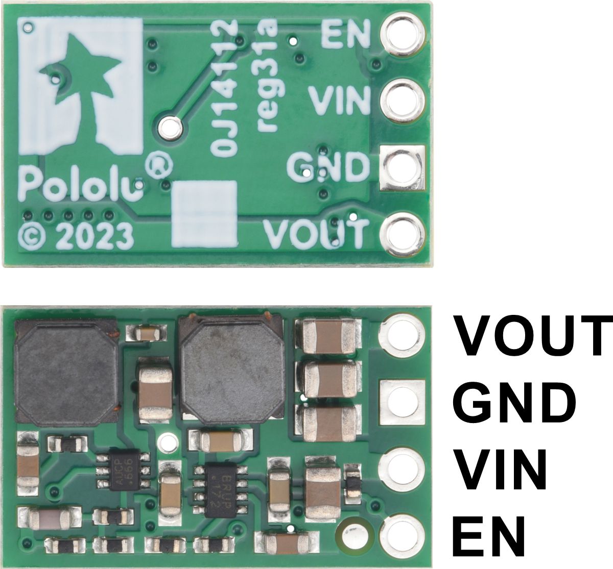 |
VOUT is the regulated output voltage. The regulator’s soft-start feature gradually ramps up the VOUT voltage on start-up to limit in-rush current draw.
The input voltage, VIN, should be between 2.7 V and 16 V when the regulator is first powered. After the regulator is running, it can continue operating down to 1.4 V. Lower inputs can shut down the voltage regulator; higher inputs can destroy the regulator, so you should ensure that noise on your input is not excessive, and you should be wary of destructive LC spikes (see the LC voltage spike section below for more information).
The regulator, which is enabled by default, can be put into a low-power sleep state by bringing the EN pin low (under 1 V). Leaving the pin disconnected or bringing the pin above 1.3 V will enable the regulator. The quiescent current draw in sleep mode is dominated by the current in the 100 kΩ pull-up resistor from ENABLE to VIN, which altogether will be between 10 µA and 15 µA per volt on VIN.
Included hardware
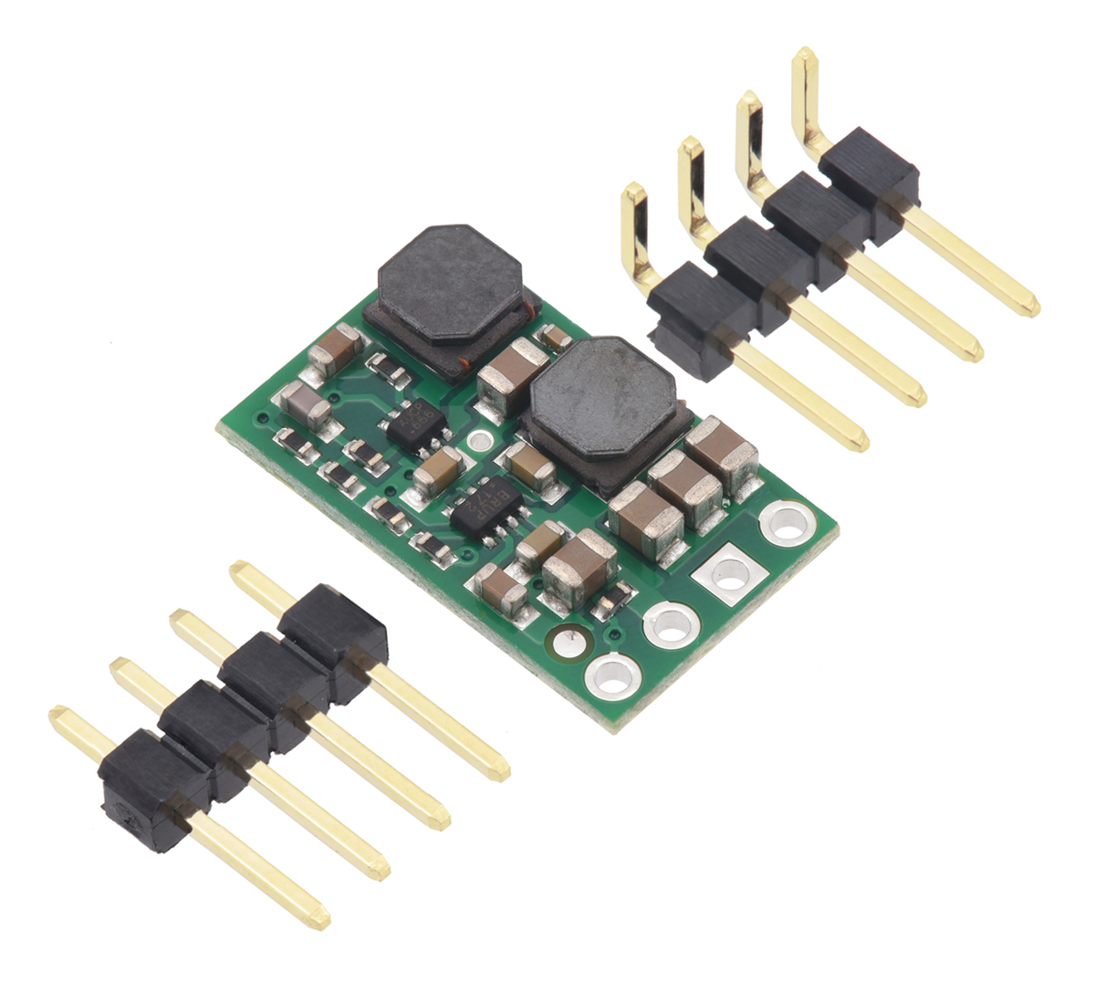 |
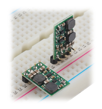
The through-holes are arranged with a 0.1″ spacing along the edge of the board for compatibility with standard solderless breadboards and perfboards and connectors that use a 0.1″ grid. You can solder wires directly to the board or solder in the included breakaway 4×1 straight male header strip or the 4×1 right-angle male header strip as desired.
 |
Typical efficiency
The efficiency of a voltage regulator, defined as (Power out)/(Power in), is an important measure of its performance, especially when battery life or heat are concerns.
 |
Maximum continuous output current
The maximum achievable output current of the regulator varies with the input voltage but also depends on other factors, including the ambient temperature, air flow, and heat sinking. The graph below shows maximum output currents that the regulators in the S8V9Fx family can deliver continuously at room temperature in still air and without additional heat sinking.
 |
During normal operation, this product can get hot enough to burn you. Take care when handling this product or other components connected to it.
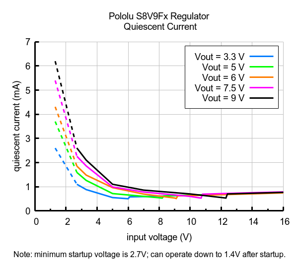
Quiescent current
The quiescent current is the current the regulator uses just to power itself, and the graph below shows this as a function of the input voltage. The module’s EN input can be driven low to put the board into a low-power state where it typically draws between 10 µA and 15 µA per volt on VIN.
 |
LC Voltage Spikes
When connecting voltage to electronic circuits, the initial rush of current can cause voltage spikes that are much higher than the input voltage. If these spikes exceed a regulator’s maximum voltage, the regulator can be destroyed. If you are connecting more than about 9 V, using power leads more than a few inches long, or using a power supply with high inductance, we recommend soldering a 33 μF or larger electrolytic capacitor close to the regulator between VIN and GND. The capacitor should be rated for at least 20 V.
More information about LC spikes can be found in our application note, Understanding Destructive LC Voltage Spikes.
People often buy this product together with:
 |
3.3V Step-Up/Step-Down Voltage Regulator S8V9F3 |
Related products


Related categories


Home | Forum | Blog | Support | Ordering Information | Lists | Distributors | BIG Order Form | About | Contact
© 2001–2025 Pololu Corporation
