Step-Down (Buck) Voltage Regulators » D30V3x Step-Down Voltage Regulators » D30V30MAx Fine-Adjust Voltage Regulators »
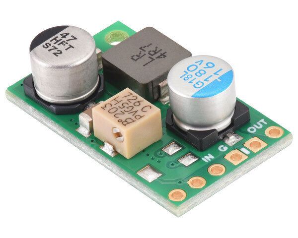
4.2-15V, 3A Fine-Adjust Step-Down Voltage Regulator D30V30MAS
| Output voltage range | Typical max output current1 | Input voltage range2 | Low-voltage cutoff |
|---|---|---|---|
| 4.2 V – 15 V | 3 A | 4.2 V – 45 V | none |
Note 1: Typical continuous output current at 30 V in and 9 V out. Actual achievable continuous output current is a function of input and output voltages and is limited by thermal dissipation. See the output current graph on the product page for more information.
Note 2: Input voltage must be higher than the output voltage and is subject to dropout voltage considerations; see the dropout voltage section of product pages for more information.
Alternatives available with variations in these parameter(s): output type Select variant…
 Compare all products in D30V30MAx Fine-Adjust Voltage Regulators.
| Description | Specs (13) | Pictures (17) | Resources (3) | FAQs (0) | On the blog (0) | Distributors (20) |
|---|
Dimensions
| Size: | 0.6″ × 1.0″ × 0.35″1 |
|---|---|
| Weight: | 3.5 g1 |
General specifications
| Minimum operating voltage: | 4.2 V2 |
|---|---|
| Maximum operating voltage: | 45 V |
| Minimum output voltage: | 4.2 V3 |
| Maximum output voltage: | 15 V3 |
| Continuous output current: | 3 A4 |
| Reverse voltage protection?: | Y5 |
| Maximum quiescent current: | 20 mA6 |
| Low-voltage cutoff: | none |
| Output type: | adjustable 4.2V-15V |
Identifying markings
| PCB dev codes: | reg32b |
|---|---|
| Other PCB markings: | 0J14388 |
Notes:
- 1
- Without included optional headers.
- 2
- Operating voltage must be higher than the set output voltage and is subject to dropout voltage considerations; see the dropout voltage graph under the description tab for more information.
- 3
- Output voltage is set by a built-in precision 11-turn potentiometer.
- 4
- Typical maximum continuous output current at 30 V in and 9 V out. Actual achievable continuous output current is a function of input and output voltages and is limited by thermal dissipation. See the output current graph under the description tab for more information.
- 5
- To -40 V. Connecting supplies over 40 V in reverse can damage the device.
- 6
- While enabled with no load. The quiescent current is a function of the input voltage, output voltage, and cutoff voltage. It is reduced to under 1 mA at higher input voltages and with correspondingly higher cutoff voltage settings or when the regulator is disabled via the enable pin. See the quiescent current graph under the description tab for more information.


